Heterogeneous Integration Technologies
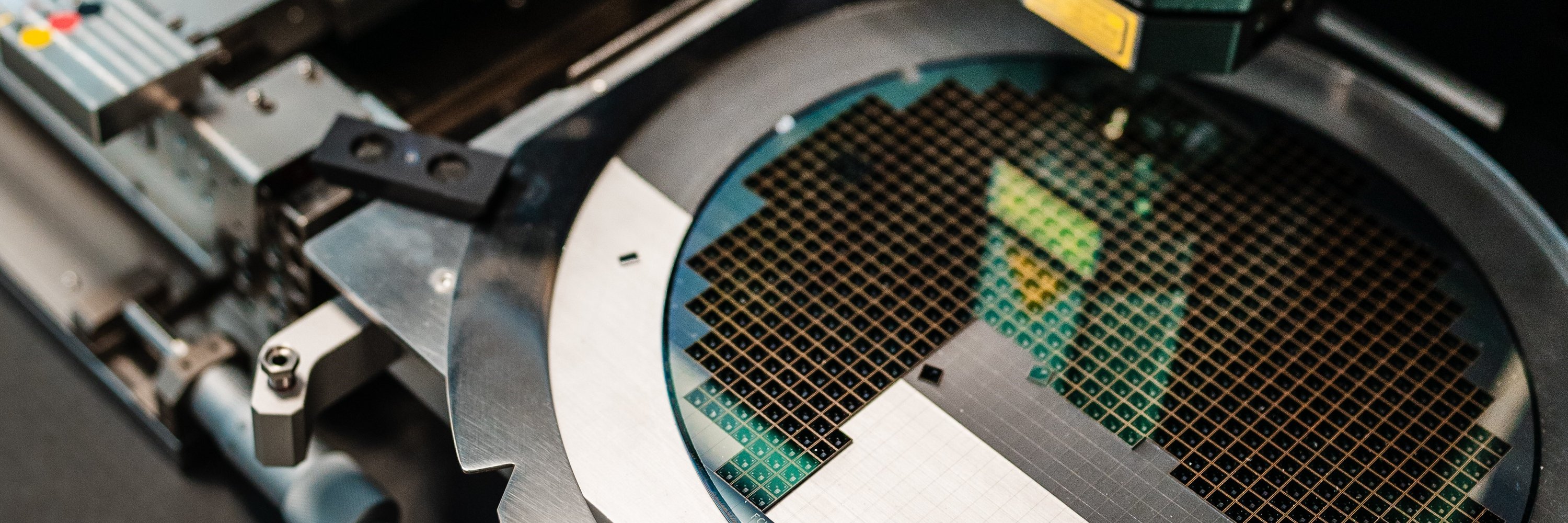
Wafer Level Packaging
SAL excels in pioneering wafer level packaging innovations, encompassing expertise in wafer bonding, wafer level hermetic packaging, wafer stacking and cutting-edge advanced chip-scale wafer level packaging solutions. Here, research and development on different wafer bonding technologies (such as anodic, adhesive, fusion & hybrid, glass frit, thermocompression bonding) is conducted and different methods for 2.5D and 3D integrations are being pursued.
3 selected publications:
- Efficient Xe Filling of MEMS Vapor Cells Empowered by Customized Triple Stack Wafer Bond Processing
- 3D Integration via D2D Bump-Less Cu Bonding with Protruded and Recessed Topographies
- Glass Frit Jetting for Advanced Wafer-Level Hermetic Packaging
Multiphysics Simulations from chip to package
Our team competences include not only single domain highly accurate fully three-dimensional simulations in the fields of fluid dynamics, thermodynamics, mechanics, and electro-magnetism but also coupling them, to properly capture the two-way interactions between different physical domains taking place in real applications. Models are developed both at the component level with three-dimensional single domain and coupled transient and steady-state calculations and at the system level, where different Reduced Order Models, reproducing different physical phenomena are connected to generate a digital tween of the system under study.
Applications: design optimization, processing and fabrication optimization, reliability studies, virtual sensing.
3 selected publications:
- Comparison of the parasitic impedances from thedrain-source path of power transistor packages atup to 2 GHz
- Multiphysics Reduced Order Modelling of a Packaged Laser Diode
- Design and Multiphysics Simulation of a PCB-Embedded-Package Enclosing a Gallium Nitride System on Chip Grown on a Novel Substrate
Photonic Packaging
With increasing demand of photonic based devices in everyday life, high precision integration and robust packaging of electro-optical system became more important. Silicon Austria Labs GmbH has developed immense expertise over decades in the field of photonics and packaging technologies. From past couple of years, photonic packaging is one of the fields which is developing rapidly under the Heterogeneous Integration Technology (HIT) unit.
Packaging photonic elements requires assembly of optical components not only in 2D, but also 3D. This is achieved through high precision pick and placement with sub-micron resolution with post placement bonding capabilities. For this, we have acquired a state-of-the-art 3D micro-assembly machine (CL 1500) from our partner FICONTEC GmbH. In addition, a two-photon lithography system (Quantum X Align) with submicron alignment accuracy from Nanoscribe GmBH, enables capability of in-package printing with high accuracy.
With the availability of state-of-the art tools and processes at hand, we offer novel and reliable solutions and processes for packaging of photonic integrated circuits and electro-optical systems from small series to scalability for high volume production such as:
- Pick and place of micro-optical components/dies
- Submicron alignment accuracy with six degrees of freedom (< 200 nm for x, y, and z)
- Bonding technologies: wire binding, flip-chip bonding
- In-package printing of micro-optical components (e.g., lenses, diffractive elements) using two-photon lithography.
- Opto-mechanical holders
- Structured optical components
3 selected publications:
- Vacuum-assisted selective adhesive imprinting for heterogeneous system integration of MOEMS devices : Automated assembly of miniaturized PM sensor
- Inkjet printed adhesives for advanced M(O)EMS packaging
- Nano-porous aluminum oxide membrane as filtration interface for optical gas sensor packaging
Chip-package characterization & analysis
Mechanical, thermal and electrical characterization of novel packaging materials and substrates are being analyzed and optimized via a wide-range of methodologies and equipment by our multi-interdisciplinary team. A few examples are listed as follows:
- Wafer-bond analysis using surface acoustic microscopy, Maszara test , IR microscopy, Shear test, Cross-sectional analysis
- Package warpage analysis: With a combination of high-precision measurements and accurate three-dimensional thermo-mechanical simulations, fabrication or working conditions of electronic components can be accurately represented to identify the development of warpage and cracks in the components due to the mismatch of thermal expansion coefficients of constitutive materials. Improvement of design and processing conditions are suggested to avoid the identified critical conditions.
- Die-attach analysis using high temperature shear testing, surface acoustic microscopy.
- Nanoindentation to obtain films material properties.
- Failure analysis using SEM, FIB, EDX and optical / IR microscopy.
3 selected publications:
- A novel interferometric characterization technique for 3D analyses at high pressures and temperatures
- Cu Pumping Analysis During Cu/SiO2 Hybrid Bonding Using In-Situ SPM Imaging
- Stress-warping relation in thin film coated wafers
Flexible Hybrid Electronics
Flexible hybrid electronics (FHE) are currently the mainstream for E-textiles, flexibles & wearables, since chip-less systems have not rendered high-performance and versatile products. In this research area, SAL develops new concepts for the integration of bare chips on flexible and stretchable substrates using flip-chip, embedding and chip-on-board technologies. The processing of the bare chips (metallization, thinning to a few microns, bumping) and the processing of the substrates (printed interconnects by electrohydrodynamic printing, inkjet printing, dispensing, PVD, aerosol, etc.) are also investigated and developed. FHE leverages the benefits of low-cost fabrication of printed electronics with high-performance silicon technologies.
3 selected publications:
- Flip chip bonding on stretchable printed substrates; the effects of stretchable material and chip encapsulation
- Direct flip-chip bonding of bare dies to polypropylene-coated paper substrates without adhesives or solders
- Flip Chip integration of ultra-thinned dies in low-cost flexible printed electronics; the effects of die thickness, encapsulation and conductive adhesives
Interconnects & Packaging materials
SAL in collaboration with industrial partners innovates and introduces new packaging materials and technologies for higher temperature, higher Power density and improved robustness such as top-side interconnects based on printing technologies (Sinterconnect ™), Cu sinter paste die-attach, Transient liquid phase die attach, Clip bonds, All-Cu interconnects and many more. Also analysis of novel adhesive materials (ACP, NCP, ICP), thermal interface, encapsulants are part of these activities.
3 selected publications:
Project highlights:
Research Program
The Austrian Advanced Packaging Center (A2PC)
From TRL 1 to TRL 7(+), our research group offers a wide range of expertise in heterogeneous integration, micro-assembly and advanced packaging. Our R&D solutions range from design, chip-package co-design and simulation to wafer-level package fabrication and characterization, and from a few prototypes to pilot production of packaged devices (CSWLP, fan-out, fan-in, SIP modules, 2.5D/3D stacked...).
Your contact person

Dr. Ali Roshanghias
Head of Research Unit Heterogeneous Integration Technologies
e-mail: contact@silicon-austria.com