- Project name: Next Gen TSV – Next generation of through-silicon via (TSV)
- Project lead: Ali Roshanghias
- Project consortium: SAL, ams-OSRAM AG
- Duration: July 2023 – June 2026
Next Gen TSV
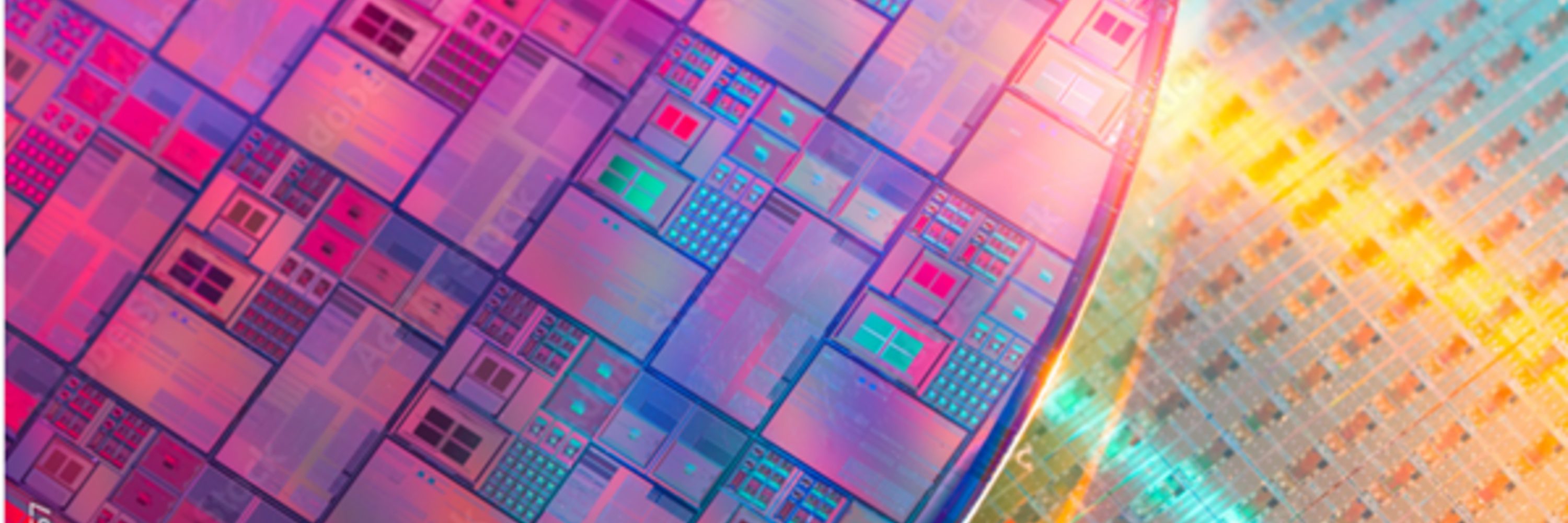
2.5 and 3D integration using through-silicon via (TSV) wafers has attracted much attention in recent years for both front-end foundries and back-end packaging. In this project, SAL and project partner ams-OSRAM AG will focus on the development of TSV wafer integration processes such as temporary bonding, via filling, thinning and debonding – specifically tailored for advanced sensor/sensing solutions. The selection of bonding and filling technologies as well as materials compatible with the TSV processing temperature is a part of this project. The assessment will cover simulation, wafer processing in the cleanroom environment as well as a reliability analysis.
Project Objectives:
- Establishing processes for TSV fabrication, protection, integration, and handling
- Proposing via filling approaches after TSV processing
- Adapting temporary bonding technologies for high-yield TSV handling
Project facts
Your contact person
Dr. Ali Roshanghias
Head of Research Unit | Heterogeneous Integration Technologies
e-mail: contact@silicon-austria.com