- Title: SURFBOND (Surface Preparation Lines for Fusion & Hybrid Bonding)
- Duration: November 2022 to October 2026
- Partner: EV Group
SURFBOND
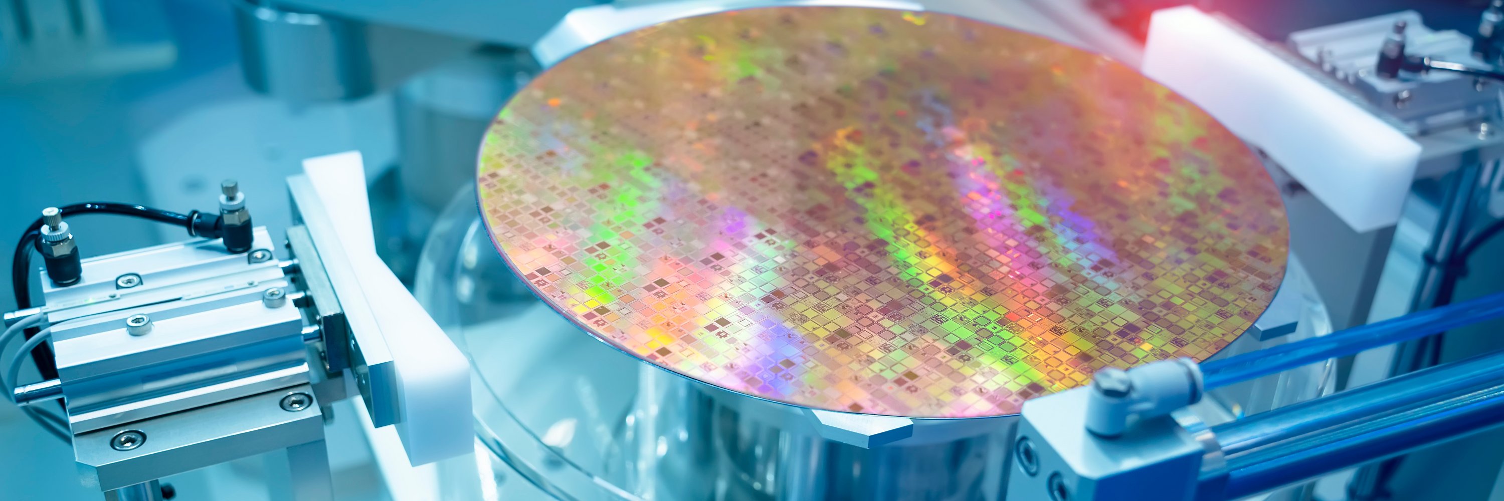
Hybrid bonding is gaining tremendous momentum in the semiconductor industry as it allows for fabricating very high-density interconnects between functional tiers via wafer-to-wafer and die-to-wafer bonding. Hybrid bonding is based on dielectric-dielectric bonds at room temperature followed by a low-temperature annealing process to establish metal-metal bonds.
SURFBOND aims to serve as a platform for developing high-end applications such as high-performance computing (HPC), AR/VR, data centers, image sensors, and many more niche applications in integrated photonics and autonomous vehicles.
Project Objectives
In the course of the SURFBOND project, partners collaborate on the development of advanced surface preparation lines for fusion and hybrid bonding. These SURFBOND processing lines comprise several process steps to prepare wafer bond surfaces including dielectric deposition, dielectric densification, CMP processing, lithography, patterning RDL, Barrier/Seed deposition, electroplating, Post CMP clean, surface activation, etc.
Project facts
Your contact person

Dr. Ali Roshanghias
Head of Research Unit | Heterogeneous Integration Technologies
e-mail: contact@silicon-austria.com
Research program
Chip2Sys is a cooperative long-term program with different cooperative SAL projects in cooperation with European key industry and scientific partners.