Manager Business Development
Microsystems


The Microsystems Research Division aims to develop beyond state-of-the-art technologies for novel micro-electromechanical systems (MEMS) and MEMS devices. In close collaboration with industrial and scientific partners, we drive transformative solutions through interdisciplinary research, connecting the dots from innovation, proof-of-concept to product prototypes.
Our research encompasses:
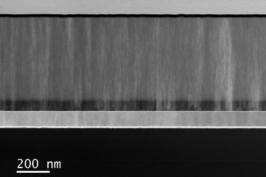
Deposition of high-quality thin films—including piezoelectric, dielectric, and metallic materials—paired with the development of innovative films, advanced characterization techniques, and real-world application testing in device structures.
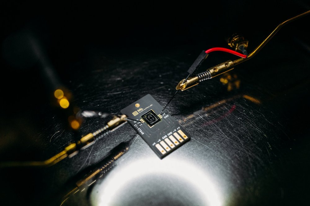
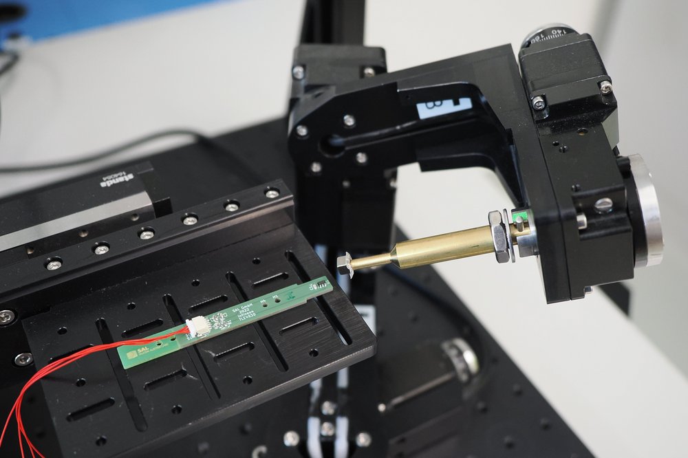
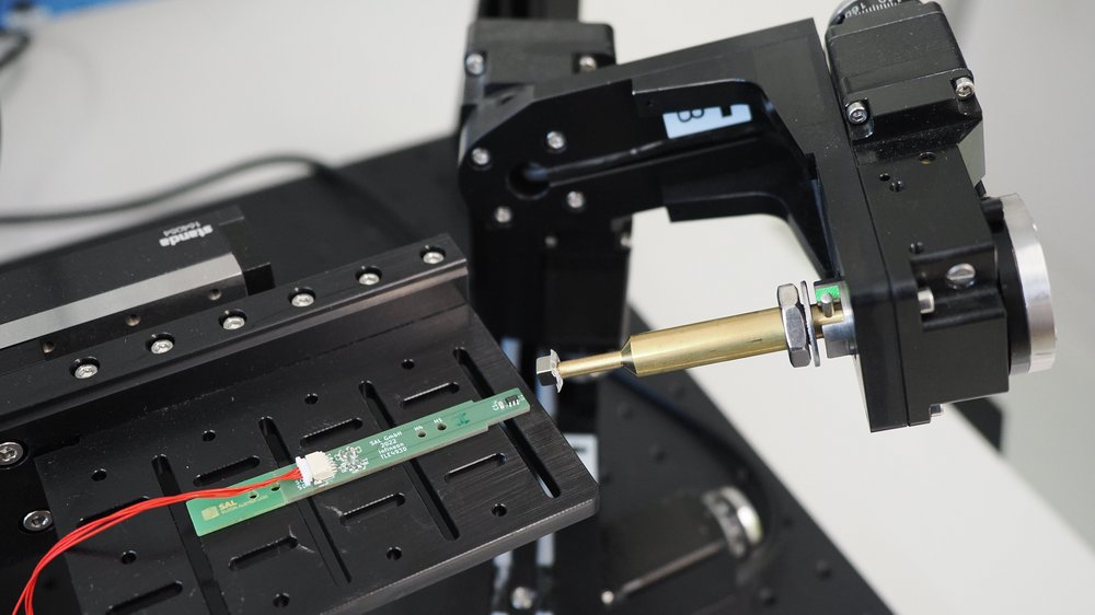
End-to-end development of next-generation piezo-based MEMS sensors and actuators — including RF-MEMS, PMUTs, micro mirror and acoustic MEMS — from concept to reality. We integrate finite element modeling, precision design, microfabrication, and rigorous testing to deliver cutting-edge solutions.
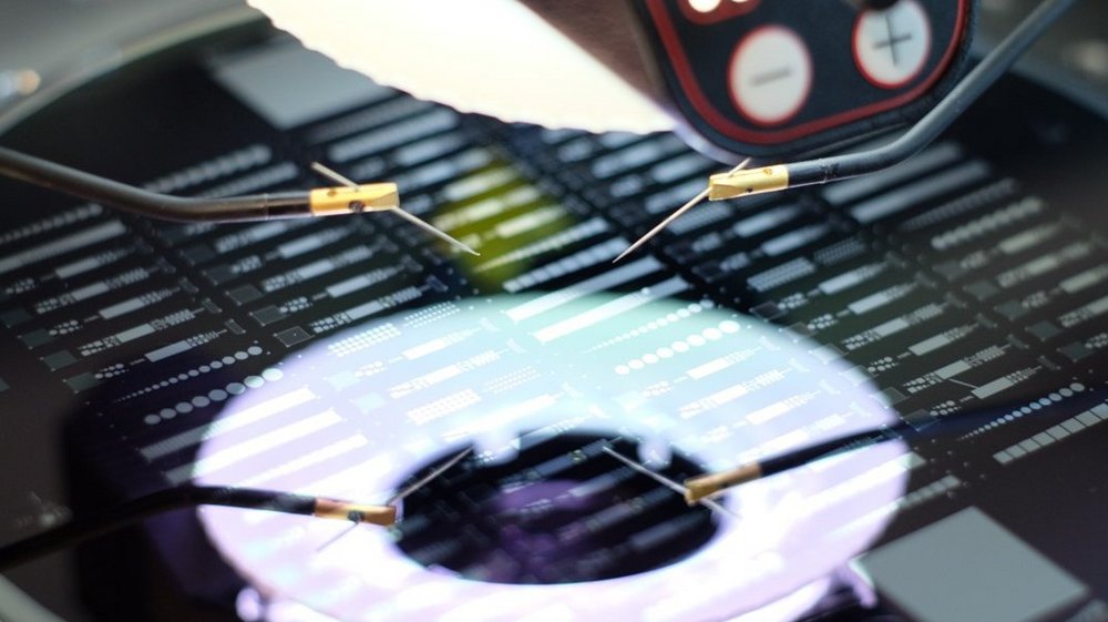
Full development from concept to prototyping of on-chip photonics-based sensors using innovative integrated photonics, meta-optics and integrated opto-microfluidics technologies. We tackle applications in remote sensing (LiDAR), 3D imaging, environmental monitoring, telecommunications and more.
Development of next-generation magnetic microsystems, sensors and magnetic position and orientation systems. We specialize in designing, fabricating and testing advanced magnetic sensors and devices—such as AMR sensors and MEMS-integrated solutions—while driving innovation through prototyping and computational modeling.
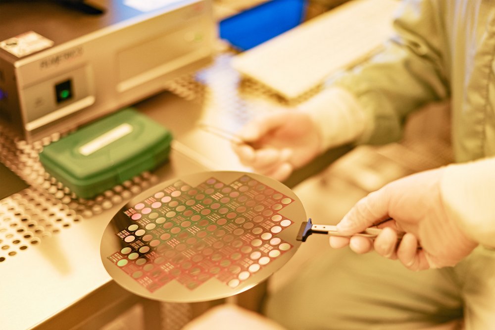
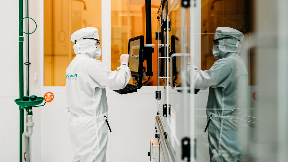
To enable beyond state-of-the-art research, it is essential to have a supporting infrastructure that fosters innovation and collaboration. Equipped with high-level equipment, our SAL MicroFab and labs provide our experts with the tools they need to push the boundaries of research forward.


Our success stories are proof to the dedication, innovation, and collaboration that drive us forward. From groundbreaking discoveries to many real-world applications, each achievement reflects our commitment to advancing knowledge and supporting our partners to be one step ahead. Explore the latest projects & success stories that have shaped different industries and pioneered transformative innovations.
Do you have any questions or would you like to know more about our services and cooperation possibilities in the field of Microsystems?
Please contact us!

Member Area
Login