Integrated Photonics Technologies
Research foci
- Photonic integrated circuit chips and systems for on-chip LiDAR, gas and chemical sensing and high-speed telecommunication applications
- Functional meta-optics, photonic MEMS devices for nanospectroscopy, 3D sensing and imaging, reconfigurable photonics
- Non-classical photonics for emerging quantum technologies
Research competencies
Our R&D team around Integrated Photonics Technologies provides interdisciplinary know-how covering theory, simulation and design, material science, nanofabrication, characterization and demonstration. The team works together closely with other research units at SAL (Cleanroom, Thin Film Technologies, Piezoelectric Microsystem Technologies, Photonic Systems and Heterogeneous Integration Technologies) to develop full device concepts and prototypes based on industrial requirements.
Photonic design and simulation
- Integrated photonic chips, both passive and active components, from single component to chip and system level
- Nano-micro-optics, optical antennas, metasurfaces for resonance, polarization, wave-propagation and wave-front control
- Developing theory and concepts for functional optical components and devices using meta-optics, non-Hermitian and non-classical optics, targeting new and multi-functionalities, smaller and flatter components for miniaturization and emerging quantum applications
- Multiphysics modeling and theory of nano-micro-opto-electro-mechanical systems (MOEMS), nano-photo-thermal systems
- Advanced approaches such as inverse design and deep learning
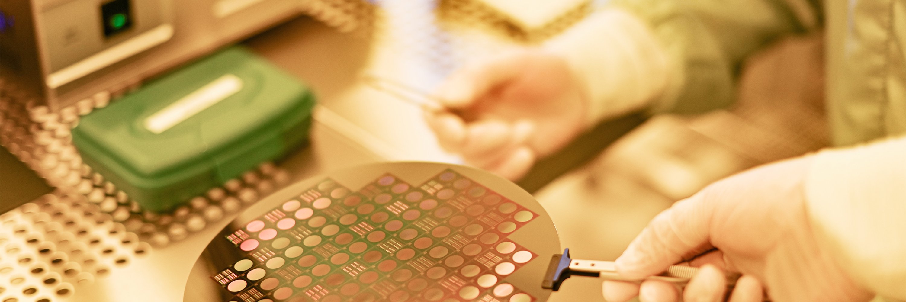
Photonic fabrication (8’’-wafer capability)
- Photonic integrated circuits
- Passive components based on SiNOI, Al(Sc)NOI platforms
- Post-processing of active components
- Wafer-level optics, meta-optics, photonic MEMS
- Low-loss optical thin-films and optical filters (oxides, nitrides, carbides, … and plasmonics)
- Molding and nanoimprint technologies for wafer-level optics (microlens, metalens, freeform optics), metasurfaces
Device characterization
Our team works in a dedicated ISO-7-cleanroom-based photonics lab equipped with state-of-the-art electronics and optical components for device characterization and demonstration.
- Sample testing: horizontal & vertical alignment, C+L band covered, component performance (loss and bandwidth), complete circuit characterization, electro-optical characteristics, complete circuit characterization
- Wafer testing: fully automatic complete batch testing and characterization by customizable routines, wafer size up to 12”, NIR and MIR available
- Lab-based environmental (gas) sensing and monitoring systems
- Opto-electronics, opto-mechanics, thermo-optics characterizations
- Optical emission spectroscopy and plasma diagnostics
Applications
- On-chip optical phased array (OPA), on-chip LiDAR for automotive applications
- On-chip gas and chemical sensors
- Nanospectroscopy and imaging
- Thermal sensors and microbolometers
- Optical emission spectroscopy for chemical characterization and plasma diagnostics.
- Customized thermal simulations (in-house engine development)
Your contact person
PD Dr. Borislav Hinkov
Team Lead Integrated Photonics Technologies
e-mail: contact@silicon-austria.com