Collaboration

Partnerships for research, development, and technology transfer – from collaborative projects to tailored innovation solutions.

About SAL

Insights into SAL’s mission, values, research activities, and contribution to Europe’s innovation ecosystem.

Thin Film Technologies

Research Focus Areas

We engineer high-performance thin films as the foundation for advanced microsystems and electronic devices.

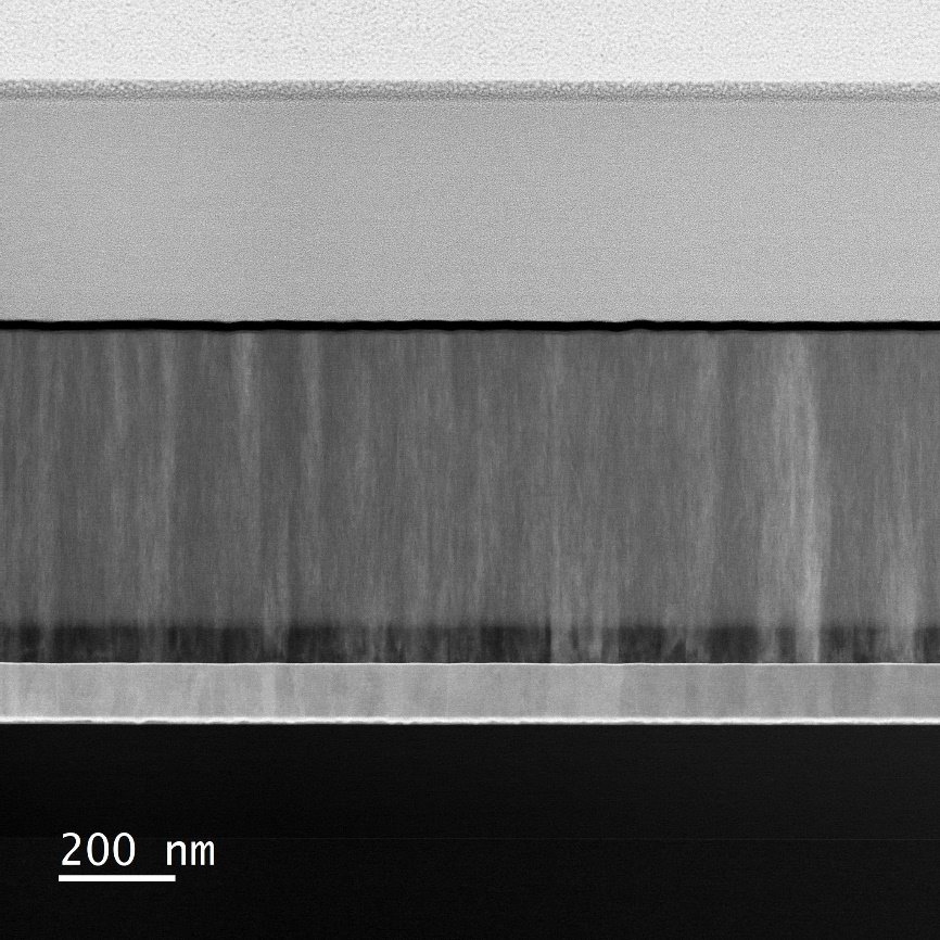
Our research focuses on the development of novel materials and scalable production processes, combining physical and chemical vapor deposition with advanced characterization techniques. We analyze material properties from atomic to macroscopic scale and optimize functional behavior such as piezoelectricity and surface interactions.

These thin films serve as key building blocks for piezoelectric, photonic, and magnetic applications across industrial and high-tech sectors.

Research Expertise

We provide comprehensive expertise in thin-film deposition, characterization, and modelling for advanced material systems.


Design & Simulation:

  • Atomistic modelling of material properties (e.g. phase stability, dielectric/piezoelectric behavior)
  • Electric field and electro-optic modelling (e.g. LiNbO₃ systems)


Fabrication:

  • Thin-film and multilayer deposition on wafers up to 200 mm
  • Physical and chemical vapor deposition of functional materials (piezoelectric, dielectric, metallic, photonic)
  • Technologies: evaporation, PECVD, PEALD, sputtering (DC, RF, HiPIMS)


Characterization & Testing:

  • Structural analysis (XRD, XRR, RSM, stress analysis)
  • Optical characterization (ellipsometry, Raman spectroscopy)
  • Electrical characterization (IV, CV, DLTS, LCR, VNA)
  • Functional testing (e.g. piezo/ferroelectric response, AFM-based methods)
  • Reliability testing (HALT) and non-standard environments (temperature, atmosphere)

Uses

Development of thin films and multilayers for piezo MEMS actuators

Development of multimaterial thin film stacks for RF MEMS and optical devices

Deposition and optimization of transparent conductive oxides for quantum applications

Development of waveguides, dielectrics and electro-optic thin films for photonic integrated circuits

Projects

WBG Pilot Line

The WBG pilot line strengthens the competitiveness of the European semiconductor industry by promoting the entire value chain and the rapid introduction of advanced wide-bandgap technologies. The focus is on WBG semiconductors such as SiC and GaN, as well as novel ultra-WBG materials for high-performance and high-frequency applications….

Surf's Up

The „Surf's Up“ project is dedicated to the development of a new generation of high-frequency filters and resonators based on a new layer transfer technology and the production of epitaxial nitride layers using magnetron sputtering....

ViTFOX

ViTFOX is an international cooperation between Europe and Korea with the goal of advancing next-generation semiconductor technologies for artificial intelligence. The project focuses on the development of „ferroelectric-enhanced“ chips that can execute Vision Transformers (ViTs) with exceptional energy efficiency of over 50 trillion operations per second per watt (TOPS/W)...

Contact

Business Development
Lisa Kainz MA
Business Development Microsystems
Graz
Head of Research Unit
Priv.-Doz. Dr. Marco Deluca
Head of Research Unit Thin Film Technologies (TFT)
Graz

Newsletter

Our Science & Stories newsletter provides the latest news, bietet aktuelle Neuigkeiten, Forschungshighlights und spannende Einblicke
von Silicon Austria Labs – direkt ins Postfach.