Advanced Wafer Level Technologies
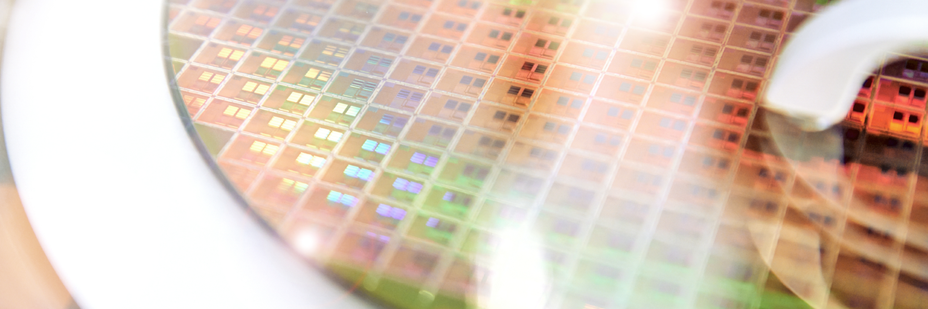
Photo: © Infineon Technologies Austria AG
Objective
To create a powerful modelling and MEMS design toolbox for advanced wafer level MEMS integration in order to improve:
- Next generation of Tire-Pressure Monitoring System (TPMS) sensors
- Innovative design and microfabrication technologies of MEMS devices
- Wafer level integration process
The main challenges and topics of investigation are:
- Modelling the influence of anodic bonding process on Tire-Pressure Monitoring System
- Modelling the charge distribution in and on the structured glass wafer
- Modelling sensitivity of electrical charges on piezo-resistive accelerometer MEMS structures
- Predict influence of wafer level MEMS technologies on any future TPMS design
Expected Results
- Predict influence of wafer level technologies on TPMS sensors
- Influence of anodic bonding process on TPMS MEMS next generation design
- Advanced simulation tool for wafer level MEMS integration
- Improvement of wafer level process technologies
Your contact person

Mohssen Moridi, PhD
Head of Research Division| Microsystems