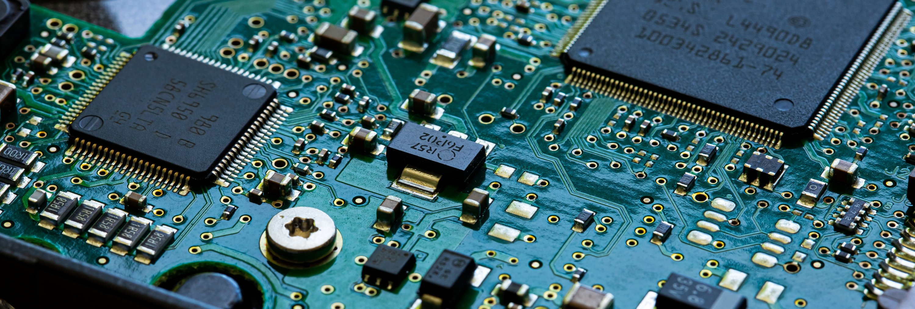
The main objectives of this project call are to develop wafer-level system-in-package (SiP) concepts for power applications with enhanced electrical performance (low parasitics, high power density, signal integrity, low resistance,..), high thermal performance (efficient heat dissipation and uniform thermal distribution) with a small footprint.
Wafer-level system in package
Partner Call open until: July 30, 2024
Project Start: Q3 2024
Objectives:
- To develop a flexible platform for wafer-level integration of muti-chips in a single package for advanced power electronics applications
- To design, simulate, and fabricate wafer-level packages rendering high power density, high performance and efficiency, compactness, and less carbon footprint
Expected results
- Development of Power System-in-Package technologies for wide-bandgap devices
- Multi-physics and multi-scale simulation models for wafer-level power packages
- Process development and wafer-level characterization of SiP power devices