Collaboration

Partnerships for research, development, and technology transfer – from collaborative projects to tailored innovation solutions.

About SAL

Insights into SAL’s mission, values, research activities, and contribution to Europe’s innovation ecosystem.

Heterogeneous Integration Technologies

Research Focus Areas

Heterogeneous Integration refers to the integration of separately manufactured components into a higher-level assembly that provides enhanced functionality and improved operating characteristics.

The research unit focuses on wafer level packaging, Multiphysics simulation from chip to package, photonic packaging, chip-package characterization, flexible hybrid electronics as well as interconnects & packaging materials.

Research Expertise

Wafer-Level-Packaging

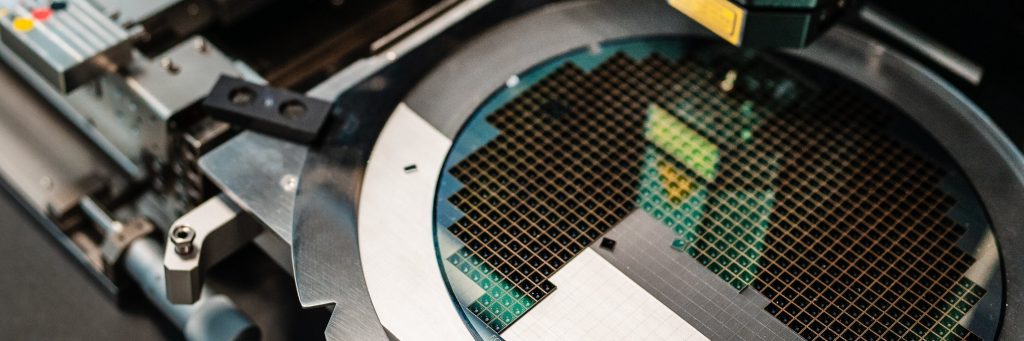
HIT specializes in wafer-level packaging, including wafer bonding, hermetic sealing, stacking, and advanced chip-scale solutions. R&D focuses on bonding technologies and 2.5D/3D integration, with two platforms: fan-out wafer-level packaging (FOWLP) and hybrid bonding.

  • 200-mm Fan-out-Wafer-Level-Packaging (FOWLP)
    • 2D/3D FOWLP with through-mold vias
    • Mold-first (silicon carrier) and RDL-first (glass carrier) approaches
    • High-density, multi-layer RDLs
    • Antenna-in-package and system-in-package solutions
    • Suitable for high-power applications
    • Automated molding and solder balling (electroplating, printing, jetting)


  • 200mm Hybrid Bonding (D2W, W2W)
    • Full process line: sputtering, etching, lithography, CMP, bonding, annealing
    • D2W, D2D, W2W bonding methods
    • Dielectric processing (SiO₂, SiN, etc.)
    • Bond analysis and metrology


Photonic Packaging

Focus on precise 2D/3D integration of electro-optical systems:

  • Wafer/chip bonding methods (anodic, eutectic, adhesive, etc.)
  • Fiber-to-PIC coupling with submicron accuracy
  • Custom PIC packaging and 3D micro-optics printing
  • Simulation and design optimization


Flexible Hybrid Electronics

Development of chip integration on flexible/stretchable substrates using flip-chip, embedding, and chip-on-board. Includes chip processing (thinning, metallization) and advanced printing techniques for interconnects.

Multiphysics Simulations

3D simulations across fluid, thermal, mechanical, and electromagnetic domains, including coupled interactions for real-world applications.

Interconnects & Packaging Materials

Innovation in materials for high temperature and power, including printed interconnects, Cu sintering, advanced die-attach, and adhesive/thermal materials analysis.

Characterization & Analysis

Mechanical, thermal, and electrical testing of packaging materials and substrates using advanced, multidisciplinary methods.

Uses

RF/mmW (Heterogeneous integration of RF transceiver)

MOEMS (hermetic /non-hermetic) and Medical (Point of care devices, IoT devices, wafer level bio-compatiable sensors)

WBG devices and Power modules

Co-packaged optics, HPC and datacenters

Projects

SURFBOND

The goal of SURF­BOND is the development of advanced surface preparation lines for fusion and hybrid bonding….

ALL2GaN

The aim of this project is to strengthen the European power electronics industry by offering an EU-originating intelligent GaN integration toolbox as a basis for applications with significantly increased material and energy efficiency. This will help meet global energy demand while simultaneously minimizing the CO2 footprint.

Contact

Business Development
Ronja Krimm MSc
Business Development HIT
Villach
Head of Research Unit
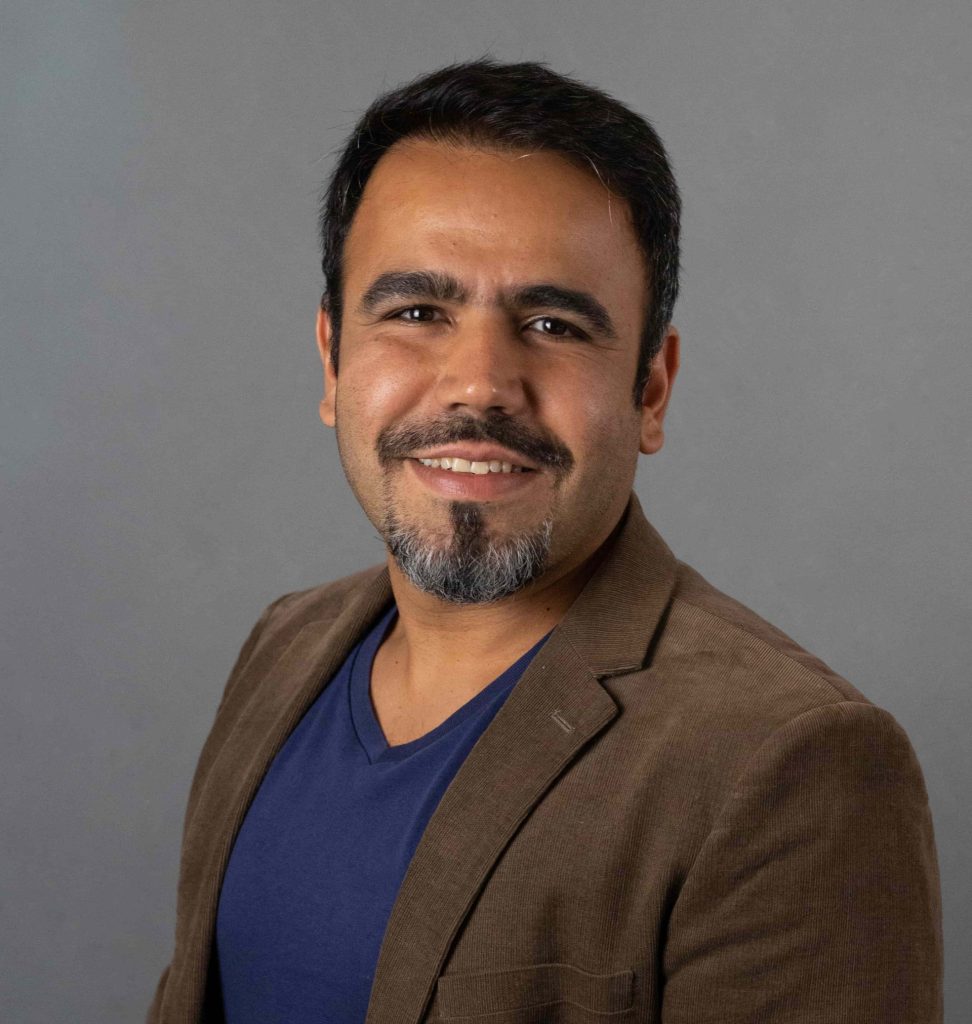
Dr. Ali Roshanghias
Head of Research Unit Heterogeneous Integration Technologies
Villach

Newsletter

Our Science & Stories newsletter provides the latest news, bietet aktuelle Neuigkeiten, Forschungshighlights und spannende Einblicke
von Silicon Austria Labs – direkt ins Postfach.