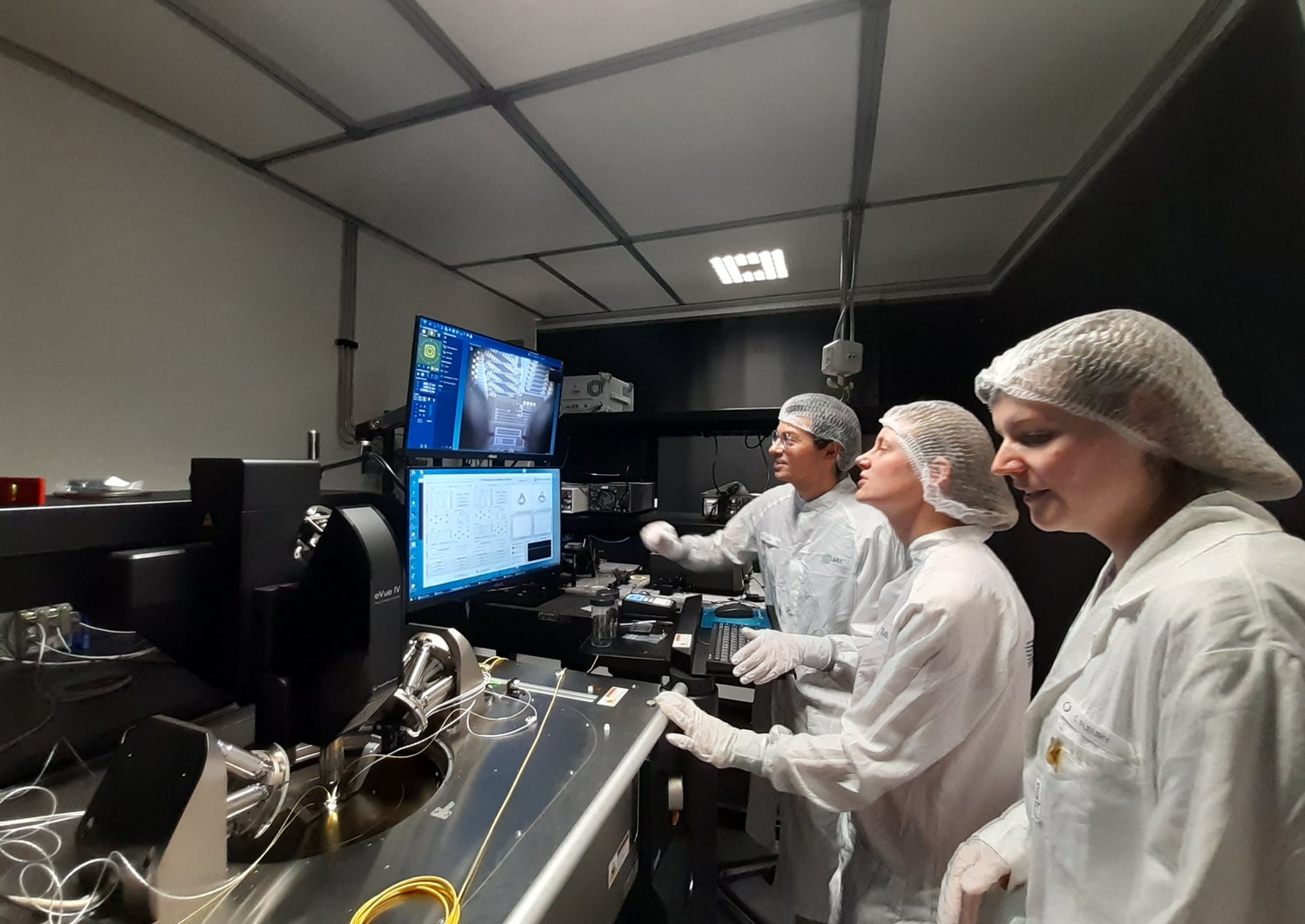
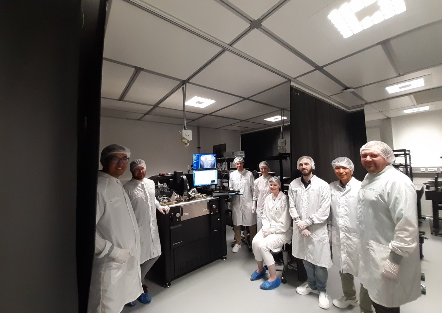
The CM300xi-SiPh 300 mm probe station is a valuable tool, able to perform opto-electrical measurement in a completely automated process. It is FormFactor’s first verified integrated measurement solution on the market that enables engineering and production-proven, optimized measurements right after installation and without further development. The CM300xi offers measurement accuracy and reliability in a solution that is completely modular – RF, DC and optical measurements in one semi-automated system, or a fully-automated dual-prober system that handles any combination of 200 mm and 300 mm wafers.
“This state-of-the-art tool has great application potential in semiconductor production. It will be of interest to companies fabricating wafer electronics and photonics, as well as universities and other RTOs, since it is the ultimate answer to the need for reliable, repeatable, automated and fast testing needed in product development cycles. Companies usually run multiple lots through the fabrication process, and they need precise measurements to characterize the wafers once the process is completed. At SAL, we now have the equipment to develop a dedicated testing recipe together with these companies, to be run on the whole lot in the shortest time and with the highest accuracy”, shares Tommaso Cassese, Senior Scientist for Integrated Photonics Technologies at SAL.
Technical details
- The CM300 consists of a 300 mm wafers compatible holder with active temperature control between -40°C to 120°C. The wafer holder can be covered by a dedicated cap to stabilize temperature and perform measurement in controlled environments (low humidity, nitrogen reach).
- A platen over the wafer chuck supports two 6-axis hexapods used for the software-controlled alignment of fibers and/or electrical probes. These hexapods, together with their fine positioning piezo-activated mover, can reach movement precision of ~2nm over a range of ~10mm in all axes, with a repeatability error of 2nm.
- The tool is equipped with several cameras used to perform passive alignment of the optical fibers/electrical probes. These cameras can also be used by the tool software to map and recognize features over the wafers in order to automatically perform coarse and fine auto alignment.
- The tool is completely controlled by a software that is both ready to use, but also open to the development of dedicated testing recipes for any application and customer