
In the manufacture of modern micro-systems, different materials are connected to one another at different temperatures. This creates mechanical tensions which can affect functionality. With precise knowledge of the behaviour of the materials, the manufacturing process can be mapped mathematically, and the resulting stresses can also be determined in the inner, metrologically inaccessible area. This forms an essential basis for the optimization of the manufacturing processes and the selection of materials.
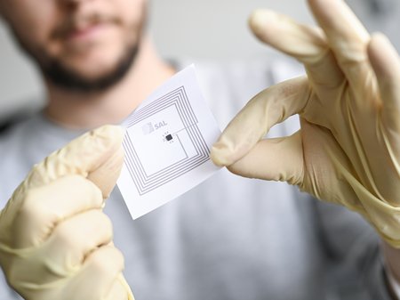
In a microsensor, an electrical circuit is thinly etched onto the surface of a silicon chip. The chip is then glued to a printed circuit board, "molded" to protect against environmental influences and connected electrically. These process steps sometimes take place at elevated temperatures. The parts expand to different degrees depending on the material and contract again when they cool down. At the same time, individual materials, such as adhesive and molding compound, initially wrap around the other - heated - parts and then solidify at a higher temperature. When the entire component is cooled down and shrinks in succession, the components warp against each other and thus generate stresses in the chip that can distort the sensor signal.
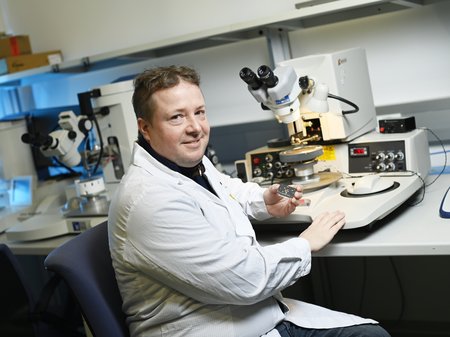
The development of the stresses on the chip was specifically investigated in the project. For this purpose, after the individual process steps, the stresses in the silicon chip were quantified with spatial resolution using Raman spectroscopy, and the behaviour of the individual materials was determined using nano indenter tests at different temperatures. At the same time, the process sequence was simulated in finite element (FEM) simulations, using the previously determined material parameters.
Impact and Effects
Knowing the interaction of different materials in the manufacturing process of embedded sensor chips allows future weak points to be identified and largely avoided when designing new applications by choosing suitable materials and coordinating the manufacturing process accordingly. This requires the most precise possible characterization of the behaviour of the materials used. The results of the first project phase enable an understanding of the interrelationships between the steps in the manufacturing process and their influence on the formation of a complex state of stress in modern microsystems. The combination of measurements and simulations is essential since the stresses occurring inside a micro-package could not be recorded by measurement alone. In the further course of the project, the findings should now be used to optimize process steps, e.g., to enable higher accuracy of the sensors. Furthermore, suitable materials can now be selected in a much more targeted manner.
The procedure exemplarily shows how important the interaction of suitable measurement methods, advanced material characterization and calculation models is for the development of micro components.
ASSIC Austrian Smart Systems Integration research Center
COMET Competence Centers for Excellent Technologies - COMET Centre (K1)
Project: Waferlevel Packages
Focus: SPO Sensor Package Optimierung, 1.4.2019 - 31.12.2022, multi firm
Project coordination: Dr. Johannes Schicker, Staff Scientist Silicon Austria Labs GmbH
Project partner: E+E Elekronik GmbH, Austria