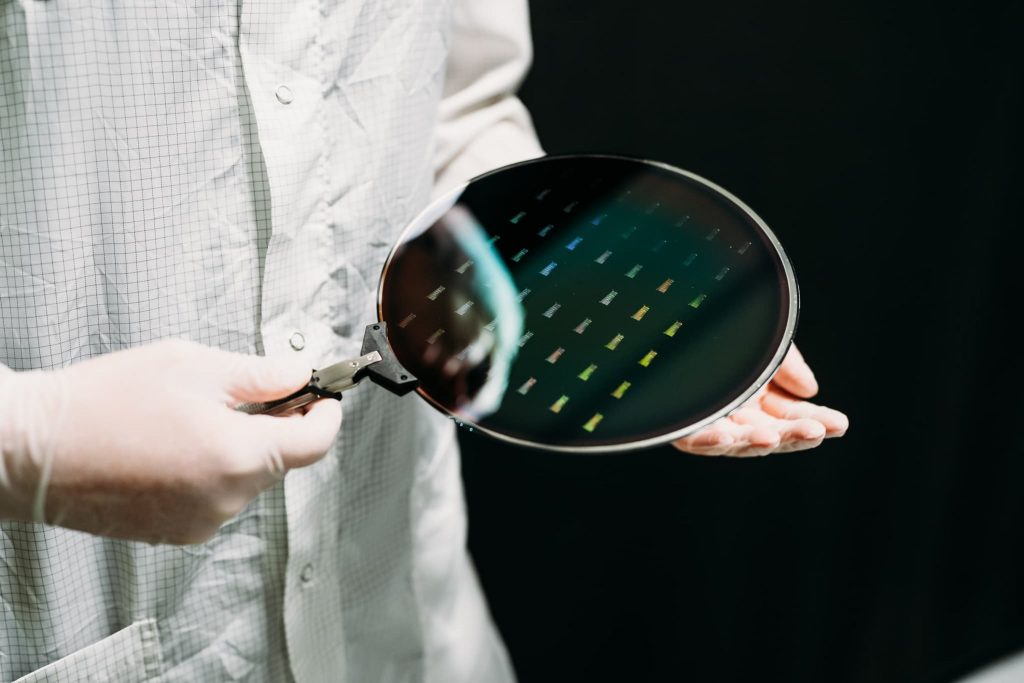
The objective of this project is to research and co-develop advanced wet etching processes for a broad range of emerging semiconductor materials relevant to next-generation applications in photonics, MEMS, quantum technologies, and wide bandgap (WBG) devices.
The project aims to establish a state-of-the-art wet processing expertise, enabling high-throughput, high-uniformity batch processing with precise control of chemical delivery, temperature, and process conditions.
Target material classes include (but are not limited to):
- Ferroelectric and electro-optic materials (e.g., Lithium Niobate, AlN)
- Wide bandgap semiconductors (e.g., SiC, GaN)
- Piezoelectric and MEMS materials (e.g., AlScN, PZT)
- Emerging quantum materials (e.g., thin films, defect-engineered materials)
- Advanced dielectric and photonic materials (e.g., TFLN, Ge)
Key challenges to be addressed include:
- Achieving high etch uniformity and repeatability at batch scale
- Controlling etch selectivity across heterogeneous material stacks
- Minimizing surface roughness and subsurface damage critical for optical and quantum performance
- Managing complex chemistries and reaction kinetics for new materials
- Enabling flexible multi-material processing within a unified platform
- Reducing chemical consumption and environmental impact
The scope of work may include:
- Provision, installation and commissioning of advanced batch wet processing equipment within SAL cleanroom by the project partner.
- Research and Co-development of wet etch processes across multiple emerging material systems
- Process parameter optimization (chemical composition, temperature, flow dynamics, wafer handling)
- Material and surface characterization (etch rate, selectivity, morphology, defectivity)
- Development of integrated process modules (etch, clean, surface conditioning)
- Implementation of process control strategies (e.g., endpoint detection, inline monitoring)
- Integration into device fabrication flows across photonics, MEMS, quantum, and WBG applications
- Correlation of process conditions with device-level performance and reliability
The project is structured as a collaborative co-development effort, inviting equipment providers to jointly research, develop and validate scalable process solutions.