During his stay Jannick is working on the improvement of the underlying materials of electronic devices, more specifically on the growth of various crystalline nitride films used in electronics. His research focuses on the usage of two separate growth methods, atomic layer deposition and magnetron sputter epitaxy (MSE). Combining these two growth methods can potentially improve materials by combining the benefits of each growth method into one process.
According to Jannick, crystals are one of the building blocks for modern electronics. Unfortunately, creating large crystals of specific materials is often not technologically or economically feasible. Therefore, very thin crystal films are deposited on top of large crystalline silicon wafers. One method for making such films is called atomic layer deposition (ALD). ALD is a great method to make nanometer thick crystal films whose thickness of a few nanometers varies minimally over large areas. “This is unique to ALD and one of the reasons we want to use it to improve our crystal growth research,” says Jannick.
Working together with a world-renowned expert
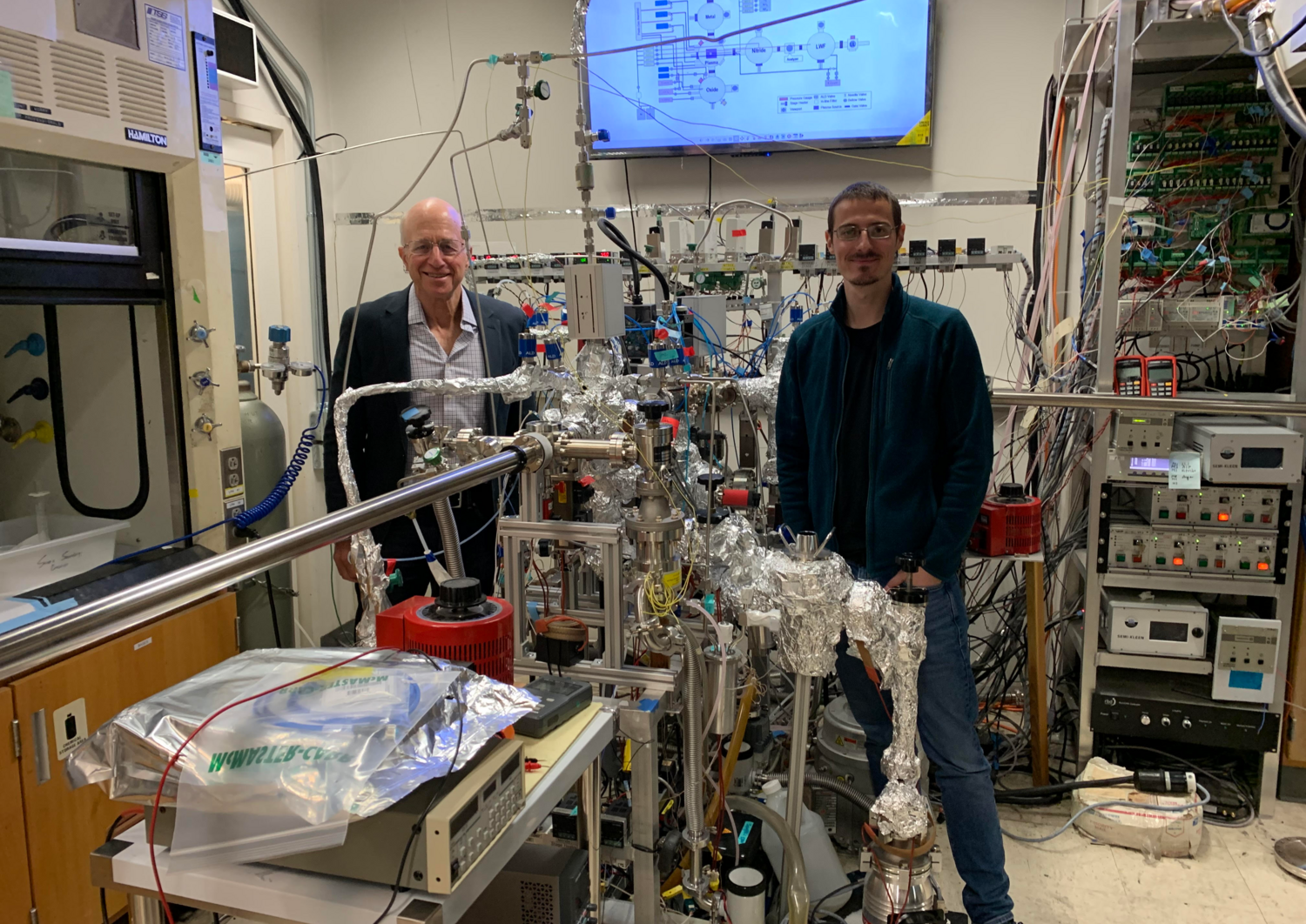
Prof. Kummel is a world-renowned expert on ALD and it’s a great milestone for one of our Junior Scientists to be working in his laboratory; an opportunity that might open doors to further international collaborative projects for SAL, too.
Prof. Kummel on Jannick’s work: “Jannick worked on the Kummel group project at UCSD on titanium nitride (TiN) atomic layer deposition and took charge of the homemade ALD system which was dedicated to this task. To operate this machine, Jannick had to master vacuum pumping, vacuum gauging, process controls, ALD valves, and ALD chemistry as well as design a new gas distribution unit (GDU). With the new GDU, Jannick was able to eliminate trace chemical vapor deposition (CVD) during ALD while maintaining record low electrical resistivity; test samples in horizontal vias have been prepared and are currently being evaluated. Jannick is writing a paper relating the TiN grain structure to electrical resistivity.”
Jannick’s thoughts on this amazing opportunity: “I am very grateful for this experience and the opportunity to learn so much about ALD in specific, and material science in general from Prof. Kummel. For me, a great benefit of working in an academic research lab that does not necessarily use industrial scale deposition tools is also learning so much about vacuum technology firsthand. This is a great addition to my work at SAL where I learn to use industrial scale tools. I am very grateful for the opportunity of being able to join one of the best PhD programs in materials science in the world that SAL provided me with!”
Jannick’s current work at the UCSD on TiN has the potential to improve the production of logic and memory devices by improving the electric wiring process. Back at SAL Villach Jannick will use the skills he acquired at UCSD primarily to work on improving the piezoelectric performance of AlN and AlScN films that are used for resonators in wireless communication or acoustic devices. This research over the next few years will also be the basis of his PhD thesis.
His plans for when he has his PhD? “Staying at SAL as a scientist to drive forward the research on ALD and sputtered thin films, of course!”