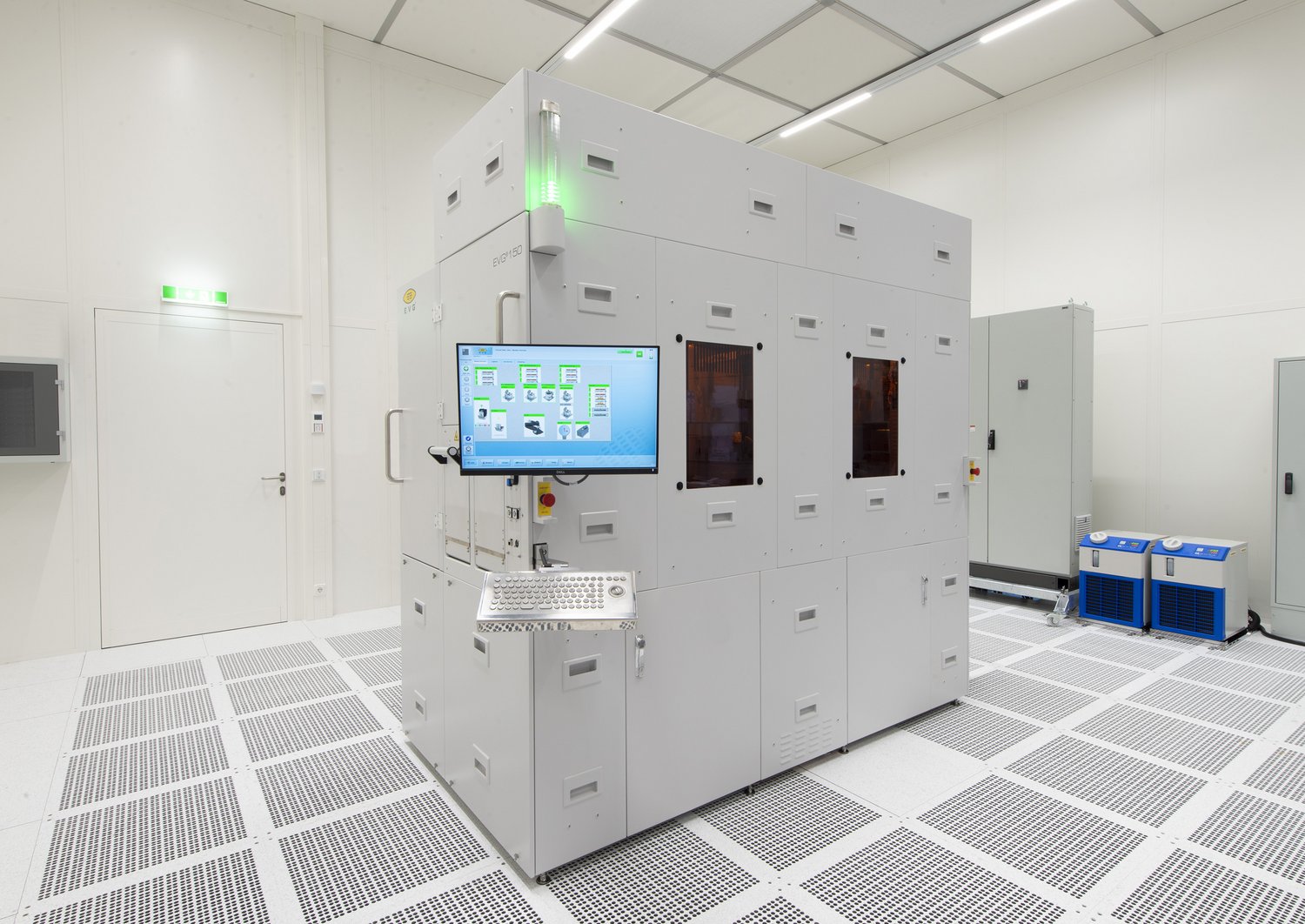
ST. FLORIAN, Austria, November 7, 2022 — EV Group (EVG), a leading provider of wafer bonding and lithography equipment for the MEMS, nanotechnology and semiconductor markets, today announced that it has strengthened its portfolio of optical lithography solutions with the unveiling of the next-generation 200-mm version of its EVG®150 automated resist processing system. The redesigned EVG150 platform includes advanced features and enhancements that provide even greater throughput (by up to 80 percent) and versatility, as well as smaller tool footprint (by nearly 50 percent), compared to the previous generation platform. The EVG150 provides reliable and high-quality coating and developing processes in a universal platform that supports a variety of devices and applications, including advanced packaging, MEMS, radio frequency (RF), 3D sensing, power electronics, and photonics. Its high throughput, flexibility and repeatability support the most demanding needs for both high-volume production and industrial development.
Company executives will be available to discuss the next-generation EVG150 resist processing system at SEMICON Europa, taking place next week at the Messe München in Munich, Germany, from November 15-18 (co-located with Electronica). Event attendees can visit EVG at Booth #C1211 to learn more.
Silicon Austria Labs, a leading research center for Electronic Based Systems (EBS), is the first customer to receive the next-generation EVG150 system. “Through our cooperative research with leading manufacturers, we develop key technologies that build the foundation for Industry 4.0, IoT, autonomous driving, cyber-physical systems (CPS), AI, smart cities, smart energy, and smart health long before they reach the market,” stated Dr. Mohssen Moridi, Head of Research Division Microsystems of Silicon Austria Labs. “The high flexibility of EVG’s next-generation EVG150 resist processing system helps pave the way for high-volume implementation of new processes and products with our development customers that fuel EBS innovation.”
Universal platform provides unprecedented flexibility
The next-generation EVG150 for 200-mm substrates maintains the industry-leading capabilities of the previous-generation platform, including: fully automated platform with customizable module configurations for spin and spray coating, developing, bake and chill; EVG’s proprietary OmniSpray® technology for conformal coating of extreme topographies; sophisticated and field-proven robot handling with dual end effector capability to ensure continuous high throughput; and wafer-edge, bowed, warped and thin-wafer handling.
New features on the next-generation EVG150 200-mm platform include:
- Up to four wet processing module spaces and up to 20 bake/chill units, enabling the processing of many more wafers simultaneously
- Singulated coat chambers, providing complete isolation of modules and virtual elimination of cross-contamination between modules
- Further redesign of modules to enable easy access to individual chambers from outside of the tool, minimizing downtime and allowing for continued tool operation when conducting chamber maintenance
- Repositioning of chambers within the platform to enable easy access to robotic handling unit to facilitate maintenance
- Image-based pre-aligner to enable on-the-fly wafer centering for faster processing
- Integration of resist and chemistry lines inside the system, reducing external cabinet space for chemistry storage and reducing tool footprint
- Integration of user interface inside the system, further reducing tool footprint
“Resist processing and patterning are the most repeated process steps in semiconductor manufacturing. EVG has built up many years of experience with these processes, including optical lithography and spin and spray coating, to address the needs of the most demanding customer requirements,” stated Dr. Thomas Glinsner, corporate technology director at EV Group. “We’ve incorporated these learnings into our next-generation EVG150 system, which has been redesigned from the ground up to provide breakthrough throughput and cost-of-ownership benefits in a universal platform that offers unsurpassed flexibility to meet the widest variety of resist processing needs.”
Product Availability
EVG is now accepting orders for the next-generation EVG150 automated resist processing system, and is offering product demonstrations at EVG’s headquarters. For more information, please visit www.evgroup.com/products/lithography/resist-processing-systems/evg150/.
About EV Group (EVG)
EV Group (EVG) is a leading supplier of equipment and process solutions for the manufacture of semiconductors, microelectromechanical systems (MEMS), compound semiconductors, power devices and nanotechnology devices. Key products include wafer bonding, thin-wafer processing, lithography/nanoimprint lithography (NIL) and metrology equipment, as well as photoresist coaters, cleaners and inspection systems. Founded in 1980, EV Group services and supports an elaborate network of global customers and partners all over the world. More information about EVG is available at www.EVGroup.com.


