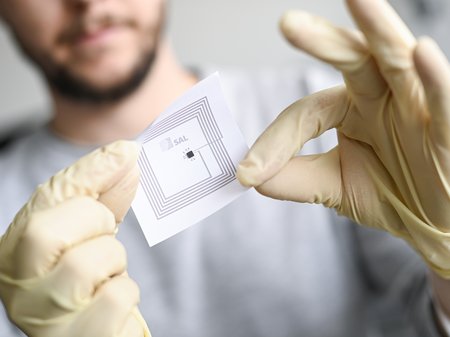

MEMS micro-scanners typically rely on silicon-based mechanical structures swinging around one or two torsional axes. An actuated reflecting area (“mirror”) in the centre of the micro-scanner is used to scan a laser beam across a line or an area. Traditionally, this actuation is achieved using electrostatic drives. To establish a seminal alternative, ASSIC researches MEMS devices based on piezoelectric actuation (“piezo MEMS”), and specifically piezo MEMS micro-mirrors, as part of its strategic research.
After successfully demonstrating 1D scanning and the advantages of piezoelectric actuation, the focus has now been put on implementing full 2D scanning. 2D scanning can be mechanically performed using specific structures like dog-bones or meanders. Such MEMS structures offer advantages in terms of performance, footprint and ease of fabrication. Moreover, piezoelectric actuation allows for 2D operation with just one mirror, while standard solutions usually require two 1D mirrors for 2D scanning. This reduces system complexity and minimises optical alignment issues.
By improving the capabilities of our piezo MEMS micromirrors and our characterization tools, we are now able to perform 2D scans and accurately assess the quality and properties of the projected patterns. Using a specific design technique developed at SAL that combines a Finite Element Method (FEM) with a custom-made algorithm we can devise complex piezoelectric actuation mechanisms. Our technique allows us to design efficient 2D micromirrors with a uniquely low power consumption and high optical scan angles along two different axes of rotation. For the fabrication of the micromirrors we collaborated with the Center for Micro and Nanofabrication, EPFL, Lausanne. This good partnership and the support from the FFG accounted for a successful outcome of this project.
Impact and effects
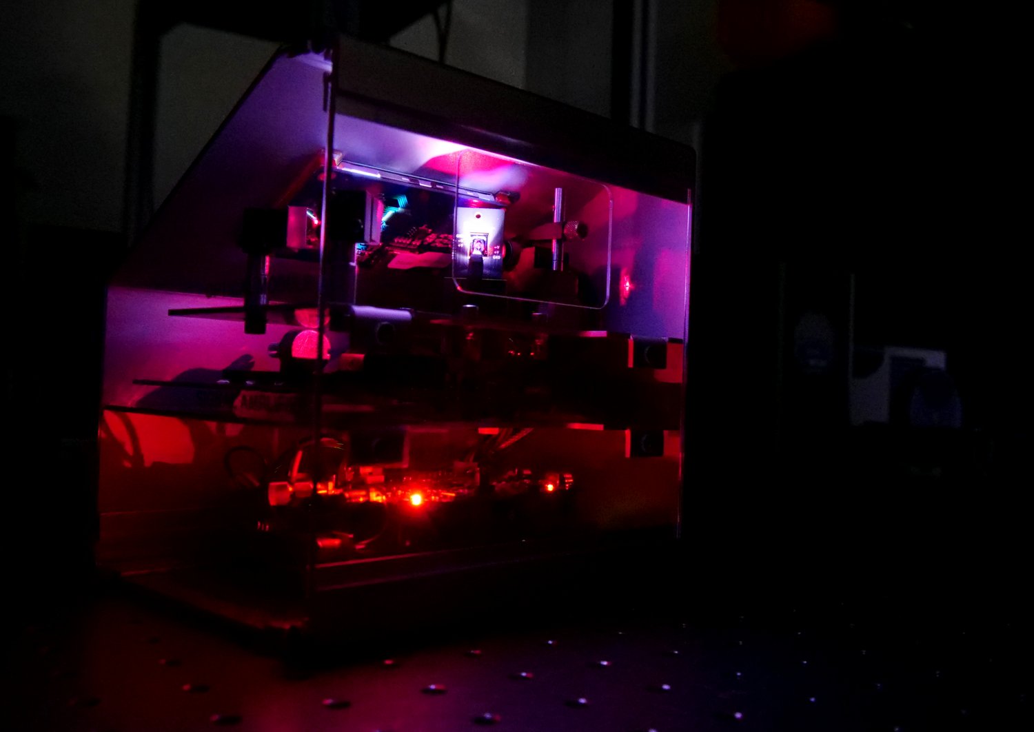
Numerous companies are currently looking for highly integrable pico-projectors. Present 2D-scanning systems are usually bulky, not energy efficient and comparatively expensive. With our 2D scanning micro-mirror using a single miniaturized structure, we aim for cost efficient, smaller and more reliable products. An in-house developed demonstrator, including a 2D micromirror and driving electronics, can display colourized shapes and can be used to assess the fundamental feasibility and limitations of a range of potential future applications. Soon, such systems could be implemented in smartphones, vehicles, or glasses.
The work was presented at the MEMS2021, the most prestigious conference in the field of microsystems. Different patent applications covering various aspects are presently being filed, and articles in international scientific journals written. Company partners already expressed their interest in our advanced technologies, and first SAL cooperative projects based on this research have recently been started. Furthermore, a strategic partnership was established with Evatec AG (CH) to jointly research and develop unique high-performance piezo thin-films in the SAL cleanroom facility located in Villach. This joint venture will enable us to become a top leader in the European research landscape for piezo thin-film materials as solutions for the next generation of integrable smart devices.
ASSIC Austrian Smart Systems Integration research Center
COMET Competence Centers for Excellent Technologies - COMET Centre (K1)
Project: Advanced MEMS Sensors and Transducers
Focus: APMM – Advanced 2D Piezo Micro Mirrors, 1.1.2019-31.12.2022, strategic research
Project coordination: Dr. Mohssen Moridi, Research Unit Head Microsystem Technologies Silicon Austria Labs GmbH