
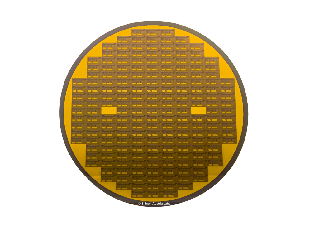
SAL has successfully processed its first 8-inch thin-film lithium niobate (TFLN) wafer for integrated photonics, marking a major milestone in European photonic innovation. Developed entirely in-house at SAL’s Villach cleanroom facility, this achievement showcases the R&D centers’ growing capabilities in advanced materials and wafer-scale photonic integration. TFLN is a key enabler for high-speed, low-loss optical components, and SAL’s achievement paves the way for scalable, high-performance photonic systems across telecom, quantum, and sensing applications.
SAL’s breakthrough in processing an 8-inch thin-film lithium niobate wafer is the result of a unified and carefully engineered process. Central to this achievement is a proprietary hard-mask deposition technique, which includes a specially developed adhesion layer to ensure high etch selectivity and process reliability. Together with this, SAL focused on the development of stitching-free electron beam lithography, followed by precision etching and post-etch cleaning steps — all optimized for large-area uniformity. The entire process was executed at SAL’s advanced Cleanroom facility in Villach, leveraging close collaboration with tool suppliers to push the boundaries of wafer-scale photonic integration.
Mohssen Moridi, Senior Executive Director states: “This achievement marks more than the successful processing of an 8-inch wafer — it is the first milestone of a broader plan to open scalable photonic manufacturing to a wider community. Starting next year, we will provide access to 8-inch TFLN MPW runs, enabling partners to benefit from faster fabrication cycles, reduced chip cost per wafer, and improved quality and yield. It’s a proud moment for our team and a significant step for Europe’s photonic ecosystem.”
Scaling photonics: SAL’s 8-inch TFLN wafer unlocks next-gen applications
The successful processing of an 8-inch TFLN wafer unlocks a broad range of opportunities across advanced photonic applications. SAL envisions this platform as a versatile enabler for technologies in telecom and datacom, detection and ranging, RF photonics, and quantum information systems. Its compatibility with other photonic platforms — such as silicon and silicon nitride — further enhances its utility, allowing hybrid integration that combines the high bandwidth and low energy-per-bit advantages of lithium niobate with the maturity and scalability of existing ecosystems.
This work has been supported by multiple funded and industrial projects, and will contribute to PIXEurope, a European photonics pilot line initiative aimed at accelerating the industrial adoption of advanced integrated photonics. This milestone positions SAL as a key enabler in the evolving European photonics landscape.
“This achievement is the result of a dedicated team effort over the past three years. We focused on developing a reliable and scalable process for thin-film lithium niobate, and while we are proud of this milestone, we recognize that there is still work ahead to refine the technology and make it accessible to a broader audience.”, adds Tommaso Cassese, Staff Scientist from the Integrated Photonics team at SAL.
Shaping the future of photonics
SAL will continue to refine its TFLN processing capabilities and explore integration with other photonic platforms. The next steps include scaling the process, engaging with industrial partners, and contributing to European initiatives such as PIXEurope to accelerate commercialization and adoption of advanced photonic technologies.
CONTACT
Lisa Kainz, MA
Business Development
Microsystems
lisa.kainz@silicon-austria.com