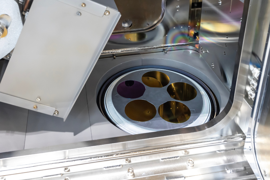
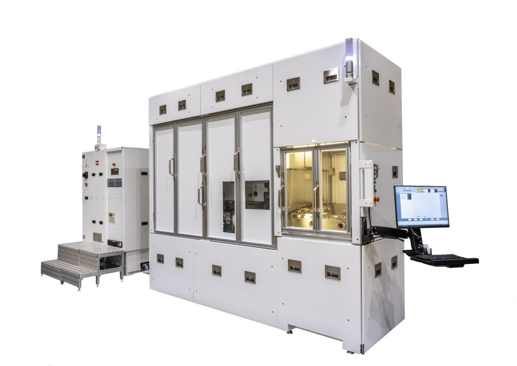
Silicon Austria Labs (SAL) and SHINCRON are joining forces to bring the first SHINCRON INACO sputter deposition platform of its kind in Europe to the SAL MicroFab in Villach. The platform adds a critical material-deposition capability to Europe’s emerging 200 mm thin-film lithium niobate (TFLN) value chain: the in-house development and control of lithium-niobate-based thin-film material stacks. This step strengthens European access to advanced lithium-niobate material capabilities and supports the scaling of next-generation technologies in integrated photonics, RF, sensing, quantum technologies and future microsystems applications.
Thin-film lithium niobate (TFLN) is emerging as a strategic material platform for next-generation high-performance technologies. Its strong electro-optic, nonlinear optical and functional properties make it highly relevant for high-speed optical communication, RF photonics, sensing, quantum technologies, co-packaged optics and advanced microsystems. However, bringing these technologies closer to industrial use requires more than isolated process steps. It requires a controlled and integrated process chain — from material deposition and stack optimization to device fabrication, integration, testing and future transfer into industrial environments.
Reliable access to high-quality, application-specific lithium-niobate-based material stacks remains a major bottleneck for scaling TFLN technologies beyond laboratory demonstrations. By bringing advanced sputter deposition capability in-house, SAL will gain deeper control over material-stack formation, including crystallinity, refractive index, stress, surface roughness, adhesion and wafer-level uniformity. This capability strengthens Europe’s emerging 200 mm TFLN value chain by reducing dependency on limited material sources, improving traceability and enabling reproducible thin-film stacks tailored to future applications.
The SHINCRON INACO system is designed as a flexible development platform for advanced sputter deposition of lithium niobate and related functional materials. Its configuration supports the exploration of new material systems and process windows across different substrates and application requirements. For SAL, this flexibility is essential: before advanced thin-film technologies can move toward industrial use, the relationship between deposition conditions, material quality and wafer-level reproducibility must be understood and controlled.
“SHINCRON is proud to contribute to SAL’s vision of establishing a 200 mm-compatible TFLN process line in Europe. As photonic technologies move closer to industrial application, success depends on the ability to understand, optimize, and reproduce the entire process chain — from material formation to wafer-level manufacturing. The INACO platform was developed with this philosophy in mind. It provides a flexible environment for process exploration, material-stack optimization, and technology maturation, while maintaining a clear pathway toward industrial manufacturing.
SHINCRON’s commitment to SAL and its partners is to help ensure that the processes developed on INACO can be transferred with confidence into robust, reproducible, and scalable manufacturing,” said Mr. Kaz Asano, Corporate Officer and Member of the Board at SHINCRON.
The collaboration combines SHINCRON’s expertise in advanced thin-film deposition equipment with SAL’s cleanroom infrastructure, process know-how and application-driven research environment. By connecting material development with wafer-level processing, device integration and future industrial transfer, the partners aim to accelerate the maturation of lithium-niobate-based thin-film technologies in Europe.
“This collaboration with SHINCRON is an important step in building a differentiated European capability for lithium-niobate-based thin-film technologies,” said Dr. Mohssen Moridi, Senior Director at Silicon Austria Labs. “With the first SHINCRON INACO platform of its kind in Europe, SAL is addressing a critical bottleneck in the TFLN value chain: reliable access to high-quality, application-specific material stacks. This is essential for Europe’s ability to move beyond isolated process steps and build deeper control over advanced thin-film materials, from deposition and process development to future integration and industrial transfer.”
With this step, SAL is moving toward a first-of-its-kind European 200 mm TFLN platform that combines material-stack development, wafer-level processing, integration, testing and future industrial transfer. By closing the gap between lithium-niobate-based thin-film deposition and downstream device fabrication, SAL can support industry partners in moving from early-stage process development toward reproducible, scalable and application-oriented thin-film technologies.
The installation will further strengthen the SAL MicroFab in Villach as a European cleanroom infrastructure for advanced thin-film processing, integrated photonics, quantum-enabling technologies, RF applications, sensing and industrially relevant microsystems. By developing material-stack expertise and process know-how directly in Europe, SAL is building the infrastructure, competence and partner network needed to move next-generation functional thin-film materials — including lithium niobate, lithium tantalate and related material systems — from material development toward scalable applications and future industrial transfer. With its 200 mm process focus and 300 mm-compatible platform concept, the system also opens a pathway toward future integration with broader wafer-level technology platforms, including CMOS-related ecosystems.