Hybrid Bonding is gaining tremendous momentum in the semiconductor industry as it allows for fabricating very high-density interconnects between functional tiers via wafer-to-wafer and die-to-wafer bonding. Hybrid bonding is based on dielectric-dielectric bonds at room temperature followed by a low-temperature annealing process to establish metal-metal bonds.
In the course of the SURFBOND project, Silicon Austria Labs (SAL) and EV Group (EVG) collaborate in the development of advanced surface preparation lines for fusion and hybrid bonding. These SURFBOND processing lines comprise several process steps to prepare wafer bond surfaces including dielectric deposition, dielectric densification, CMP processing, lithography, patterning RDL, Barrier / Seed deposition, electroplating, Post CMP clean, surface activation, etc.
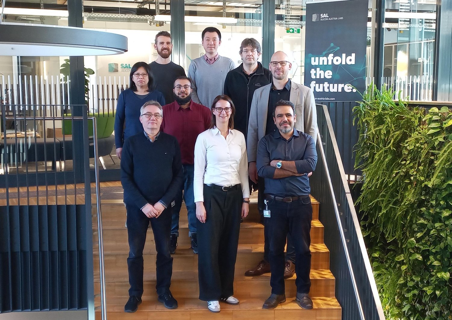
Now, the 1st year review meeting of this project was successfully held in Villach. Furthermore, we had a tour of SAL’s new cleanroom where the SURFBOND lines are being installed. SURFBOND aims to serve as a platform for developing high-end applications such as high-performance computing (HPC), AR/VR, data centers, image sensors, and many more niche applications in integrated photonics and autonomous vehicles