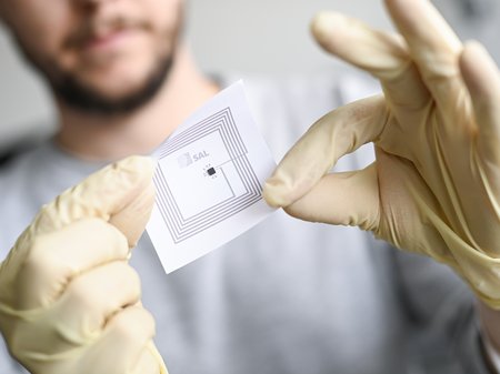

Besides increasing wafer diameters, R&D in power semiconductor processing is dominated by shrinking device thicknesses to some 10 μm. With this, mechanical stresses introduced during processing increasingly become a problem, first in the handling of warped (thin) wafers, and subsequently in premature device failures. With stresses introduced by a variety of factors all along the processing chain, from layer deposition and structuring past wafer thinning to chip separation, understanding the root causes, and quantifying the relative contributions becomes increasingly important.
Yet, current quality control only measures the external forces required to mechanically break a statistically meaningful number of sample chips, providing only information as to the when a chip fails, but not why. Increasing production quality and yield requirements in combination with calls for greener manufacturing eliminating preventable waste call for an alternative that is capable of directly and rapidly measuring absolute mechanical stress in silicon and relate that to predicting the probability of a chip failing.
Vibrational Raman spectroscopy (RS) is known to be capable of directly measuring stress in various materials, including monocrystalline silicon (sc-Si). By measuring the relative shift of a Raman-active Si phonon peak, it is possible to quantify the stress in silicon, with tensile strains shifting the centre wavelength to lower frequencies while compressive stresses result in higher centre frequencies. The challenge was now to establish that as a tool for pinpointing chip stress and resulting early failure to specific processes and process steps.
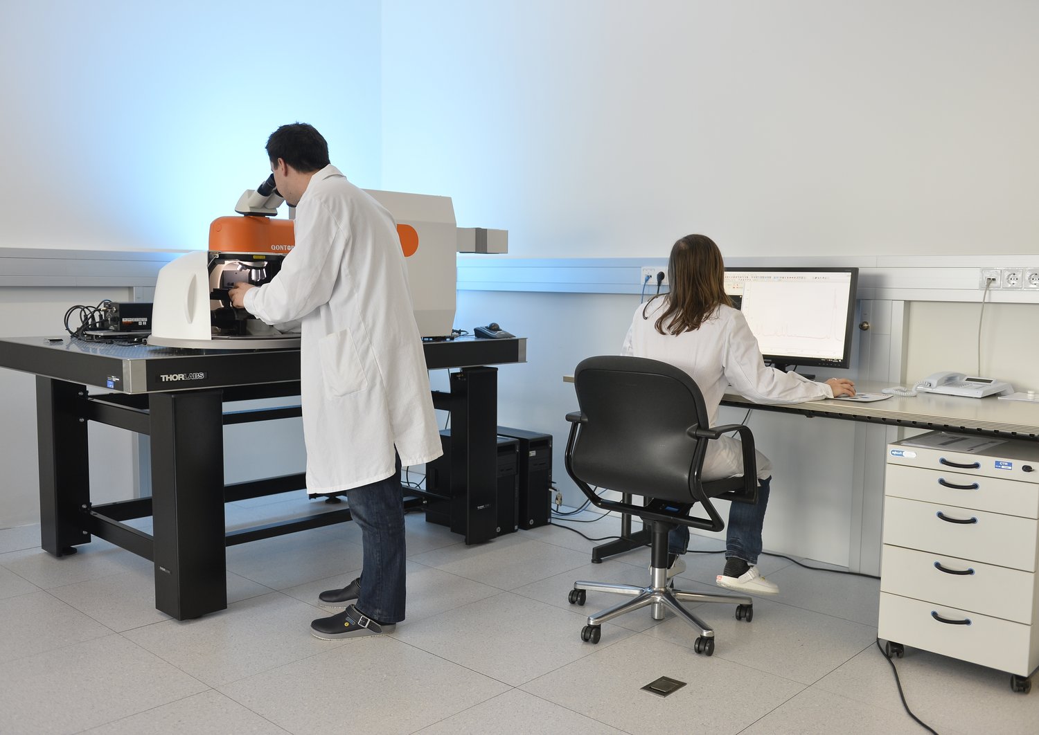
In a joint effort with Infineon Technologies, samples were extracted from various stages of an established manufacturing process and analysed using a Raman research instrument (Renishaw Qontor) that offers a wide range of options, including multiple excitation wavelengths and polarisation-dependent analysis. In addition to a direct analysis, the data was subjected to a correlation analysis, matching it against chip breakage results.
Shown exemplarily for chip dicing, the Raman data clearly correlate with breaking strengths. In this case, mechanical dicing introduces the lowest stress and thus achieves the highest breaking strengths. Laser dicing performed clearly worse, with a reproducible impact of the thermal budget on both inner stresses and the effective overall breaking strengths.
Impact and effects
With the introduction of Raman spectroscopy as a nondestructive, fast, and contact-free method to R&D in semiconductor processing, a metrology tool was established that can reliably and reproducibly measure mechanical stresses directly, without damaging or even touching the samples. Future work will now focus on an inline measurement system that can measure the stress at-line or even in-line during processing, to provide immediate feedback to the operator and optimize process parameters and yield.
ASSIC Austrian Smart Systems Integration research Center
COMET Competence Centers for Excellent Technologies - COMET Centre (K1)
Project: Smart Sensor Systems for Micro- and Nano-sized Contaminants
Focus: MiNAS - Non-destructive spectroscopic micro- and nano-analysis of semiconductor materials and structures, 1.1.2019 - 31.12.2022, multi firm
Project coordination: Martin De Biasio, M.Sc., Senior Scientist Silicon Austria Labs GmbH
Project Partner: Infineon Technologies, Austria & Germany